
PRODUCTS
- 首頁
- 經營品牌
- E+H Metrology GmbH
- 自動化設備
- Global Nanoscope
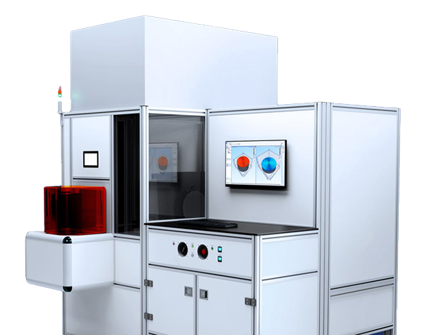
Global Nanoscope
E+H
The Global Nanoscope (GNS) offers cutting-edge technology with key benefits:
。Full-Surface Measurement: Eliminates stitching for a competitive edge.
。High Speed: Measures substrates in 30 seconds, with 3D evaluations in 1-2 minutes.
。True Nanotopography: Delivers reliable nanometer-height resolution.
。Vibration-Resistant: Functions reliably in dynamic production environments.
。Cost-Effective: Low maintenance costs with durable components.
。Fully Automatic & Integratable: Seamlessly fits into any workflow.
。Comprehensive Support: Expert guidance and local distributor assistance throughout its lifecycle.
The application possibilities of the GNS are as comprehensive as its range of features.
。Any surface evaluation and classification is possible quickly and contact-free with the Global Nanoscope, e.g.
- Identification of dimples
- defect analysis
- Peak-to-valley analysis of surfaces
。Wafer fabrication: For fast and comprehensive process control of many production steps during wafer fabrication (e.g. grinding, polishing)
。Chip fabrication: The Global Nanoscope is particularly well suited for rapid incoming inspection of wafers to be processed.
。Analysis according to SEMI M43 Guide for Reporting Wafer Nanotopography: Determine standard-compliant detail values in the nanometer range.
。Glass & optical Industry: All reflective surfaces are suitable for nanometer precision measurement via Global Nanoscope.
Our proprietary and AMA-approved Advanced Makyoh technology goes one step further than was previously measurable:
。E+H Metrology Advanced Makyoh: Conventional Makyoh systems provide two-dimensional grayscale images showing irregularities on a surface. However, the actual height of such surface structures is crucial for industrial applications, especially in sensitive processes such as wafer production. Conventional Makyoh systems therefore measure purely qualitatively: typically, standard Makyoh images are quite blurry.
。The system based on E+H Advanced Makyoh, however, determines real height information of the surface in one measurement process.
。Classical 2D Makyoh images in 2D are also provided by the Global Nanoscope: but with a very high resolution. Our system is therefore capable of both qualitative and quantitative measurement.
。The Advanced Makyoh image data can be further processed as desired: For inspection, for complex 3D analysis or for evaluation by existing IT landscapes and control systems.
Characteristics
。Thickness
。Flatness (TTV)
| Wafer Diameter | up to 300 mm |
| Dynamic range | gradient: ±0.14°, bow up to 100 μm |
| Lateral resolution | 110 μm |
| Resolution (height) | 1 nm (typically, with small bow below 50 μm) |
| Standard Deviation | 1 σ ≤ 1 nm (n=31) |
| Edge Exclusion | 1mm (Notch + Mount) |
| Measuring time | 30 sec |
| Calculation time | 1 - 2 minutes |
| Vibrational stability | VC-A (~50 μm/s [4 - 80 Hz]) |
| Typical data size per Wafer | 50 MB (500 MB full analysis data) |