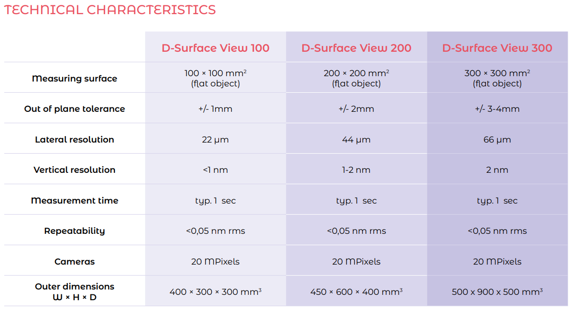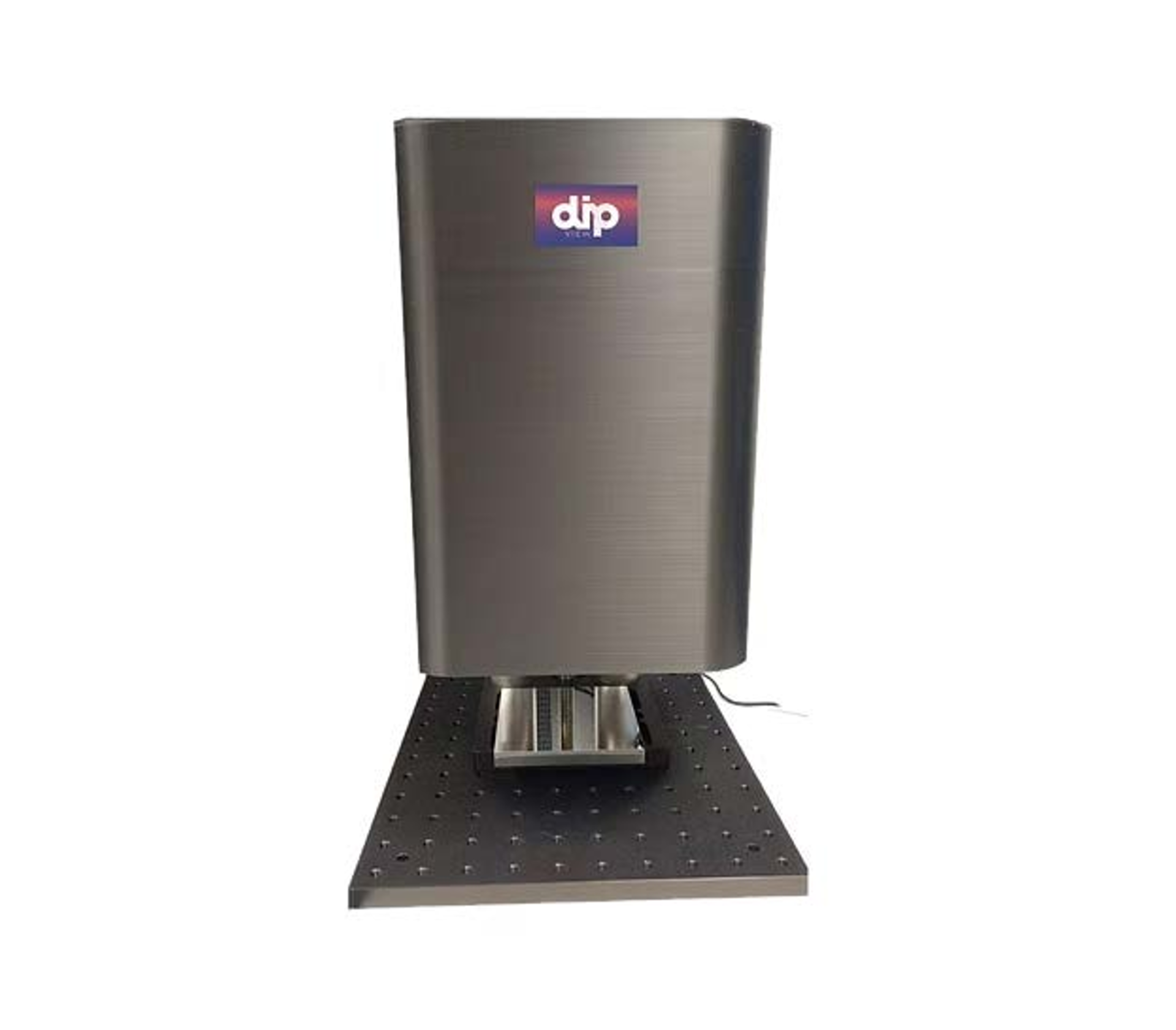
D-Surface View
DipView
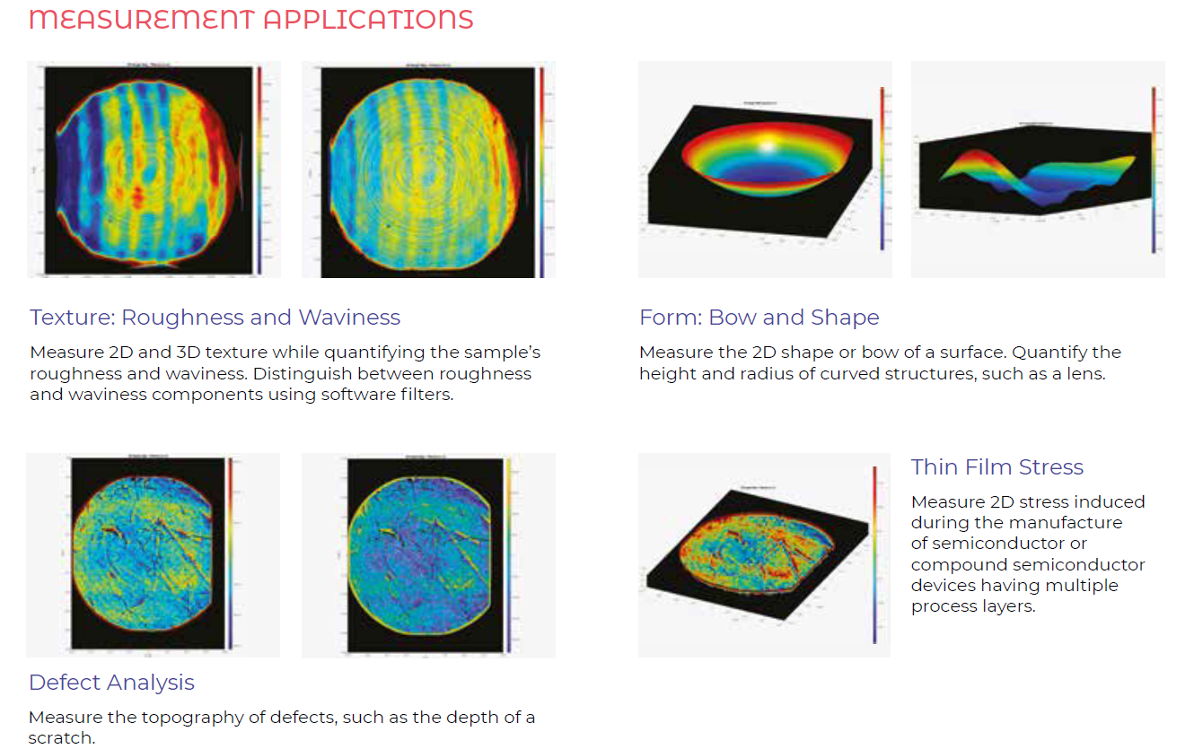
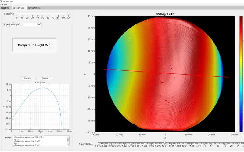
Warpage measurement
D-Surface View provides a FULL SURFACE warpage measurement in one single acquisition. Users can extract critical parameters such as Bow, Warp, TTv, LTv in a few seconds.
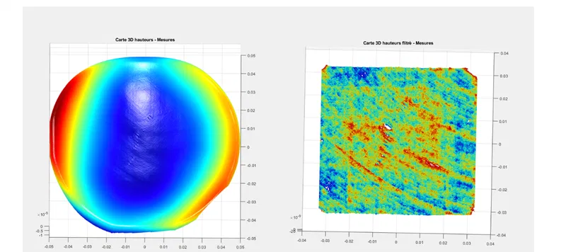
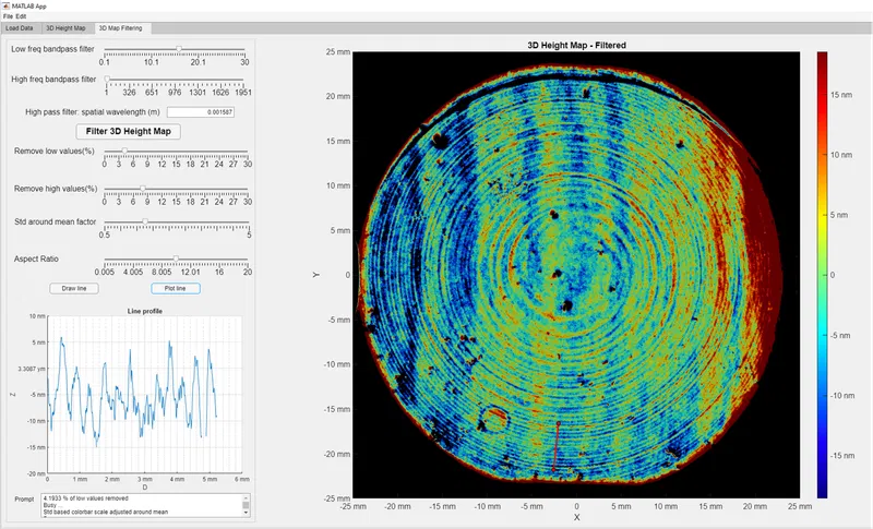
Nano-Topography measurement
D-Surface View can explore Nano-topograpgy characteristics and detect polishing inhomogeneities or other nanometer height defects. With powerful fourrier transform filters users can visualise short frequency and high frequency defect patterns.
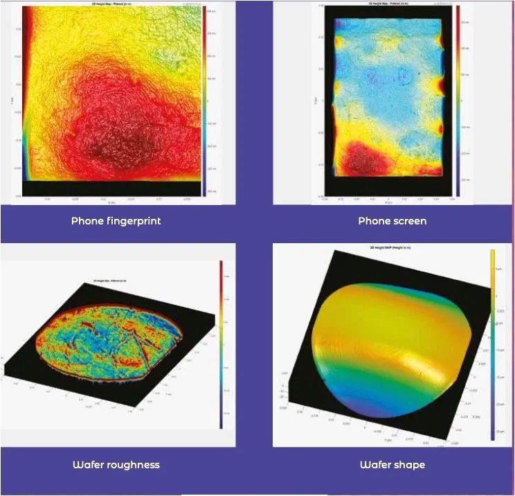
Data Analytics on a large range of measurement
In one single high resolution image and pure static acquisition D-Surface View can extract from mm level down to nm level in a few seconds, users can explore the full field image at the required resolution and process through Data Analytics algorithms and Open data formats.