PRODUCTS
- 首頁
- 經營品牌
- Hologenix Inc.
- 缺陷檢查設備
- Defect Detection on Ultra-Flat Wafers (Magic Mirror™)
Defect Detection on Ultra-Flat Wafers (Magic Mirror™)
Hologenix
The Magic Mirror™ is useful for detecting problems with many types of wafer processes:
• Polishing
• Epitaxy
• Oxidation, Diffusion, CVD
• Post Implant Annealing, RTP
• CMP
• SOI
New Capabilities
• High Resolution Camera and Optical Components – 5 MegaPixel Camera
• IR (Infrared) Camera and Optics
• Long Focal Length Version – Greater Detection Capability for Shallow Defects
• Computer Controlled Optical Settings
• Latest Automation Capabilities – Edge handling, Wafer Sorting
Optical Technique
• Halogen Lamp with Band-Pass Filter
• Series of Lenses Create Broad Beam Collimated Light Column
• Parallel Rays of Light Reflect Perpendicular to the Polished Surface – Min. 3% reflectivity required
• Reflected Rays Projected onto De-focused CCD Detector.
Software and Computer Control of Optics
Optics are controlled via a Software Interface:
• Brightness
• Sensitivity
Settings can be stored in a recipe and easily recalled
No operator involvement needed.

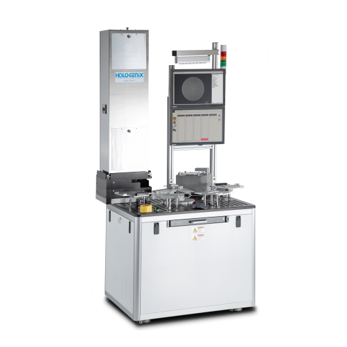
Hologenix YIS-MM-2N Magic Mirror™
2, 3 or 4 Cassette Wafer Surface Inspection Systems
• Automatic Defect Detection with Hologenix ADDS Image Processing Software
• Detection Sensitivity better than 0.05 Micron Depth with <1M-100M Radius of Curvature using the Proprietary Magic Mirror™ Method
• Defect Size Range: 0.4 μm height difference over a 10 mm lateral distance to 0.05 μm over a 0.5 mm lateral distance
• Adjustable Defect Detection and Classification Recipes
• Non-Contact Notch, Flat-Finding and Centering Technology
• 150-200 mm Wafer Inspection
• Throughput: Approx. 150 Wafers per Hour
• 2, 3 or 4 cassettes or SMIF pods. The -2N model #is for 2 open cassettes
• Class 1 Clean Room Compatible
• Windows 10 Environment
• Standalone Sorter Capability with optional OCR

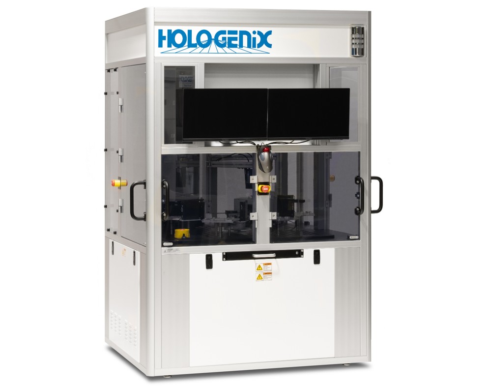
300mm Magic Mirror™ YIS-300SP-2
Automated Defect Detection System
• Detection Sensitivity better than 0.05 Microns Depth
• 13 or 25 Wafer Capacity FOUP or Open Cassette
• Class 0.1 Mini-Environment
• 200-300 mm Wafer Sizes
• Edge Grip Wafer Handling
• Non-contact Notch Finder & Aligner
• SECS II - GEM
• Optional OCR
• Windows 10 Based Defect Detection Software - ADDS
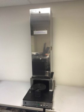
200mm or 300m Magic Mirror™ YIS-200SP or YIS-300SP
Defect Detection System – Manual System
• Detection Sensitivity better than 0.05 Micron Depth
• Full View and 3.5X Zoom
• 200SP – Up to 200 mm Wafer Sizes
• 300SP – Up to 300mm Wafer Sizes
• Computer Controlled Sensitivity
• Computer Controlled Intensity
• Manual Loading
• Rotating Wafer Chuck
• Broad Beam Illumination with Narrow Band-Pass Filtered White Lamp
• Defect Detection and Image Enhancement Software

